16-bit color VGA adapter
[Fall 2023] Our final project demonstrated the display of RGB565 16-bit color (also called high color) over VGA using a Raspberry Pi Pico. To the authors’ knowledge, this is the first ever implementation of RGB565 on a Pico above 320x240 resolutionwithout the use of an SPI display with a built-in frame buffer. In other words, our display driver stores the entire frame buffer in SRAM onboard the Pico, and our monitor does not buffer any pixel data written to it. Importantly, our adapter can inter
- Suitable forB.Tech/B.E Embedded Systems students
- Build time4-6 weeks
- LevelBeginner
- Available atAjvika Labs, Kakinada
About this project
Introduction
Our final project demonstrated the display of RGB565 16-bit color (also called high color) over VGA using a Raspberry Pi Pico. To the authors’ knowledge, this is the first ever implementation of RGB565 on a Pico above 320x240 resolution
without the use of an SPI display with a built-in frame buffer
. In other words, our display driver stores the entire frame buffer in SRAM onboard the Pico, and our monitor does not buffer any pixel data written to it. Importantly, our adapter can interface directly with any commercially available VGA display without any additional proprietary hardware.
Various optimizations and configurations were required, both from hardware and software, to conform to the strict hardware requirements of the Pico.
High Level Design
Inspiration
Our inspiration for this project came from a video made by YouTuber “Ben Eater” titled “The world’s worst video card?” (Video link:
https://youtu.be/l7rce6IQDWs?si=WuT67nbaP6HmP-60
). In this series, Eater built a functional VGA display adapter exclusively from analog and TTL components including shift registers, adders, binary counters, and EEPROM. Although the adapter was very basic, capable of only displaying a maximum of 64 colors at a resolution of 100x75 pixels, it was still a significant achievement in the breadboard computer community. We sought to expand on this and similar projects to build a video display adapter but with much more capability.
Previous Work
While defining our project scope, we researched two prior groups from Cornell who had attempted similar VGA display adapters to our own.
Professors van Adams and Land successfully designed a 320x240 pixel resolution VGA driver at 8-bit color for the Pico RP2040 (
https://people.ece.cornell.edu/land/courses/ece4760/RP2040/C_SDK_vga256/index_vga_256.html
). The driver utilized programmable I/O (PIO) state machines to control 10 GPIO pins without necessitating CPU clock cycles, which significantly improved its performance. Color information was stored pixel-by-pixel in a frame buffer onboard the Pico’s SRAM, and pushed out via Direct Memory Access (DMA) channels. Together, PIO and DMA alleviated the CPU from having to move data between memory and GPIO, which allowed the video card to refresh the screen at 60 frames per second (FPS.) Their design did not depend on an SPI display with an in-built frame buffer.
A group led by Whitmore-Wilson in the Fall 2021 cohort of ECE 4760 designed a 320x200 pixel resolution VGA driver with four colors for the PIC32 series microcontroller. Similar to van Adams and Land, they used DMA channels to push processed color data from the microcontroller out to the display. Unfortunately, Whitmore-Wilson were unable to get more than four colors working on their driver, despite using a display capable of displaying over 262,000 colors. In addition, their design required the use of a SPI-capable screen with an in-built frame buffer, which reduced the interoperability of their driver design for standard VGA applications.
Design Description
The final design was an RGB565 VGA-compatible display interface with an output resolution of 400x300 pixels. Two PIO state machines onboard the Pico were chained to DMA channels responsible for pushing color data out of 16 GPIO pins, one per color bit. Two additional state machines were used to generate the H-sync and V-sync video timing signals required by the VGA specification. Additionally, an asynchronous communication standard was added on top of a generic UART channel to allow us to design programs on other platforms to control our VGA display adapter. For example, we modified an open source ray tracing library to run on a laptop and wrapped the library in a UART application to allow the laptop to send the individual pixel values to the VGA adapter, so that we could visualize the ray-traced scene in real-time.
Hardware Design
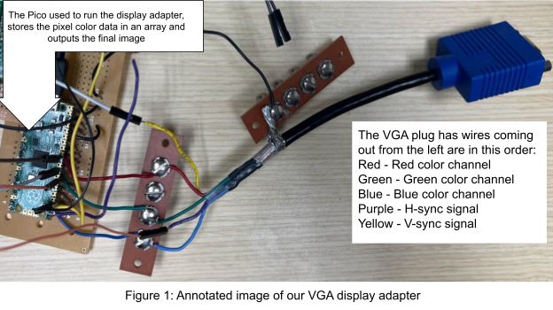
The primary piece of hardware used was a single Raspberry Pi Pico microcontroller. The Pico contained a dual-core RP2040 microprocessor which we overclocked to 270 MHz, and also packaged 264 KB of onboard SRAM. The Pico was responsible for the timing of a valid VGA signal. Figure 1 below is an annotated image of our display adapter which shows the Pico and the wires which connect the Pico to a VGA plug, which can be connected to a monitor.
The second piece of hardware was a set of digital-to-analog converters (DAC) built using resistors. We soldered together a R-2R ladder, which is a DAC built exclusively from resistors of resistance R (in this case, 330 Ω) and 2R (in this case, 680 Ω) because if the resistors are cherry-picked such that each resistor’s resistance is close to the required R or 2R rating, then this type of DAC is much more accurate than a binary weighted resistor DAC. Three DACs were constructed, one per color. Because our target color space was 16-bit, also called RGB 565, a 5-bit DAC was used for the red channel, a 6-bit DAC for the green channel, and a 5-bit DAC for the blue channel. Figure 2 below is an annotated image of our DACs.
We note that although 680 Ω is not an exact doubling of the resistance of 330 Ω, we specifically cherry-picked our resistors to be close to an exact doubling. For example, in the red channel DAC, 5% tolerance resistors were selected from a large 330 Ω bin to be close to 335 Ω, and 5% tolerance resistors were selected from a large 680 Ω bin to be close to 670 Ω. Below is a table of our selected resistors, and their total tolerances from each other.
Red Channel
Green Channel
Blue Channel
R:
335.7 Ω,
335.2 Ω,
335.8 Ω,
335.0 Ω
2R:
671.0 Ω,
670.8 Ω,
671.2 Ω,
671.0 Ω,
670.4 Ω,
670.5 Ω
R:
333.4 Ω,
333.2 Ω,
333.8 Ω,
333.0 Ω
333.0 Ω
2R:
667.0 Ω,
666.8 Ω,
666.7 Ω,
667.2 Ω,
667.0 Ω,
666.4 Ω,
666.6 Ω
R:
334.2 Ω,
334.2 Ω,
334.3 Ω,
334.7 Ω
2R:
667.8 Ω,
668.8 Ω,
668.2 Ω,
668.0 Ω,
668.1 Ω,
668.7 Ω
The DACs were each soldered to the Pico through perfboard. We could not use a solderless breadboard because the frequencies required for our circuit were over 30 MHz, and the breadboards available had too high of parasitic capacitances to support those high frequencies.
A detailed schematic of our DAC design can be found in Appendix C of this page.
Software Design
To demonstrate the Pico’s ability to display 16-bit color, our program allowed for the display of both dynamic and static images. A UART communication channel was established to allow for external sources (in our case, either another Pico or a laptop) to push an image frame to the Pico VGA adapter for display. Additionally, six 400x300 resolution images were loaded into the 2MB of onboard flash, and could be cycled and shown to the display via a push button. To introduce as little memory overhead as possible, the
unsigned short
data type (which has a range of 16 bits, equivalent to the 16-bit color range) was used to store a single pixel’s color value.
VGA Driver Theory – Resolution and Timing
The majority of the project was spent on interfacing the Pico with a VGA display by optimizing our VGA driver for high-speed GPIO connectivity. But first, we would like to explain more about the VGA specification and how we realized the complex timing scheme in code.
We dissected van Adams and Land’s codebase for 8-bit color at 320x240 pixel resolutions. According to
TinyVGA
, a 320x240 resolution could be achieved by “downsampling” a standard 640x480 resolution signal in half by both the horizontal (called a scanline) and vertical (called a frame) directions. In other words, by sending the same color value twice for every pixel in a scanline, and by duplicating each scanline twice, a monitor is essentially displaying a 320x240 color image while operating at a higher 640x480 resolution. This process is known as pixel doubling or scanline duplication.
The 400x300 resolution could be achieved with a similar doubling procedure from the native 800x600 resolution. According to TinyVGA, the 800x600 timing standard utilized a 36 MHz pixel clock. This was the frequency used to send a single color pixel to the display. Additionally, the VGA signal itself was broken down into a few portions. For example in each scanline, the first 24 pixels drawn (the front porch) are not shown on screen, but the subsequent 800 pixels create the width of the visible area of the display. Next, 128 pixels are drawn off-screen (the back porch) and then a final 72 pixel “H-sync” pulse is initiated. During the sync pulse, the voltage of the color lines and the pulse itself must be shorted to ground. This gives the display time to “sync-up” the pixel drawing signal with the display, and also gives the display time to erase (blank) the screen. A similar sequence of front porch, visible area, back porch, and V-sync pulse is performed in the vertical direction. But because VGA scans lines from top to bottom, the V-sync pulse only needs to initiate at the end of every frame.
Therefore, the software design theory was to write a simple loop to trigger once per tick of a 36 MHz clock. Upon receiving the trigger, the loop would index into a large array containing every pixel value for the display and get the value of a 16-bit integer. It would interpret the integer as 16 binary digits and output the integer along 16 GPIO pins for color, one pin per digit. Additionally, another clock would generate the H-sync and V-sync pulses, and a loop would trigger every time the H-sync and V-sync signals should be grounded. At this time, the binary value “0” was written to all 16 GPIO color pins, and held until the pulse ended. Then, the binary values for the next color would be written to the color
pins
. Additionally, to perform scanline duplication, another loop or flag would control if the previous scanline had been duplicated. If the flag was not set, then the last scanline had not been duplicated, so duplicate the last scanline and set the flag. Otherwise, the last scanline was duplicated, so move on
Technologies used
Hardware components
- RP2040
- Raspberry Pi Pico
- PIC32
- VGA display
- IMU
- DAC
- EEPROM
Software & tools
- C
- Arduino IDE
Project demo video
What you get
- Working project / hardware kit, tested before delivery
- Complete source code with explanation
- Project demo and guidance for your viva
- Project report, PPT and IEEE paper support (on request)
Related Embedded Systems projects

Gas Leakage Detector Using Arduino
A budget-friendly LPG gas leak detector built with an Arduino and MQ-5 gas sensor, triggering a buzzer and LED when unsafe gas levels are de...
View project
Simple Alarm System
A beginner-friendly home alarm with PIR motion sensing, keypad PIN entry, and separate entry/exit timing delays, built to be easy to expand.
View project
Ultrasonic Sensor Project with Arduino UNO Q
A beginner-friendly first Arduino UNO Q project: a servo-swept ultrasonic sensor that renders a live sweeping radar display in a web browser...
View project
3D Audio Localization
[Fall 2025] We designed a real-time embedded system that localizes sound sources in three dimensions and visualizes them live using a four-m...
View project